The polarization switching in nanoscale with an anisotropic 2D magnetic semiconductor
R. Komar, A. Łopion, K. Mosina, A. Söll, Z. Sofer, W. Pacuski, C. Faugeras, P. Kossacki, T. Kazimierczuk
 Solid State Communications 397, 115798 (2025)
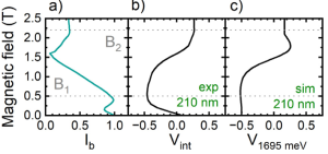
We present a proof-of-concept device demonstrating the feasibility to control the light polarization using the properties of the magnetic 2D materials. The studied structure consists of a diluted magnetic semiconductor quantum well and a thin layer of CrSBr. We show that by application of the external field we can switch the sign of the polarization of the emitted light. The theoretical modeling confirms that such a switching is a direct consequence of a colossal shift of the exciton lines observed in the high energy range of the CrSBr spectra. Owing to this mechanism, the full rotation of the polarization state can be realized in a layer as thin as few hundred nanometers.
Coherent imaging and dynamics of excitons in MoSe2 monolayers epitaxially grown on hexagonal boron nitride
K.E. Połczyńska, S. Le Denmat, T. Taniguchi, K. Watanabe, M. Potemski, P. Kossacki, W. Pacuski, and J. Kasprzak
Nanoscale 15, 694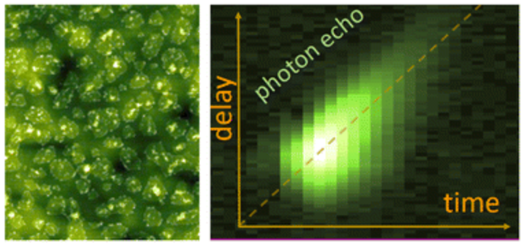 1-6946 (2023)
Using four-wave mixing microscopy, we measure the coherent response and ultrafast dynamics of excitons and trions in MoSe2 monolayers grown by molecular beam epitaxy on thin films of hexagonal boron nitride. We assess inhomogeneous and homogeneous broadenings in the transition spectral lineshape. The impact of phonons on the homogeneous dephasing is inferred via the temperature dependence of the dephasing. Four-wave mixing mapping, combined with atomic force microscopy, reveals spatial correlations between exciton oscillator strength, inhomogeneous broadening and the sample morphology. The quality of the coherent optical response of epitaxially grown transition metal dichalcogenides now becomes comparable to the samples produced by mechanical exfoliation, enabling the coherent nonlinear spectroscopy of innovative materials, like magnetic layers or Janus semiconductors.
Hybrid electroluminescent devices composed of (In, Ga) N micro-LEDs and monolayers of transition metal dichalcogenides
K. Oreszczuk, J. Sławińska, A. Rodek, M. Potemski, Cz. Skierbiszewski, and P. Kossacki
Nanoscale 14, 17271-17276 (2022)
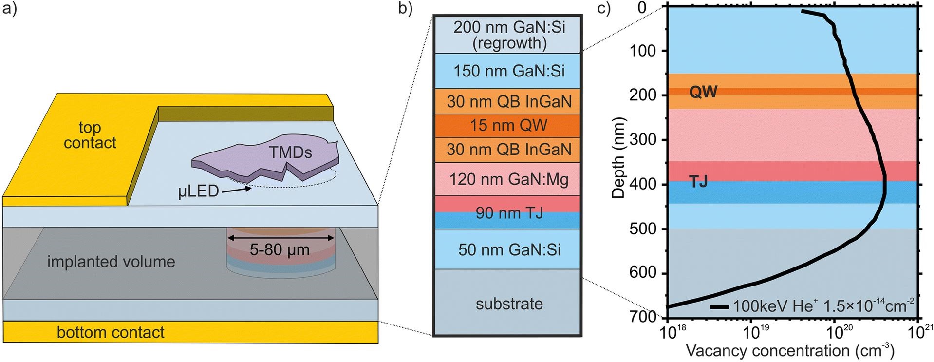
We demonstrate a novel electroluminescence device in which GaN-based u-LEDs are used to trigger the emission spectra of monolayers of transition metal dichalcogenides, which are deposited directly on the μ-LED surface. A special μ-LED design enables the operation of our structures even within the limit of low temperatures. A device equipped with a selected WSe2 monolayer flake is shown to act as a stand-alone, electrically driven single-photon source.
Magnetic ion relaxation time distribution within a quantum well
A. Łopion, A. Bogucki, W. Krasnicki, K. E. Połczynska, W. Pacuski, T. Kazimierczuk , A. Golnik, and P. Kossacki
 Phys. Rev. B 106,165309 (2022)
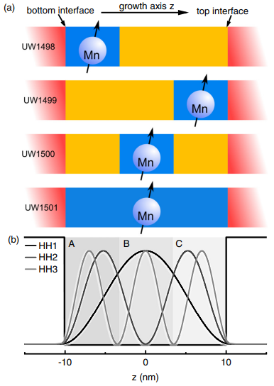
Time-resolved optically detected magnetic resonance (ODMR) is a valuable technique to study the local deformation of the crystal lattice around magnetic ion as well as the ion spin-relaxation time. Here we utilize selective Mn doping to additionally enhance the inherent locality of the ODMR technique. We present the time-resolved ODMR studies of single (Cd,Mg)Te/(Cd,Mn)Te quantum wells with manganese ions located at different positions along the growth axis—in the center or on the sides of the quantum well. We observe that spin-lattice relaxation of Mn2+ significantly depends on the ion-carrier wave-function overlap at low-magnetic fields. Interestingly, the effect is clearly observed despite very low carrier density, which suggests the potential for control of the Mn2+ ion relaxation rate by means of the electric field in future experiments.
Angle-resolved optically detected magnetic resonance as a tool for strain determination in nanostructures
A. Bogucki, M. Goryca, A. Łopion, W. Pacuski, K. E. Połczyńska, J. Z. Domagała, M. Tokarczyk, T. Fąs, A. Golnik, and P. Kossacki
Phys. Rev. B 105, 075412 (2022)
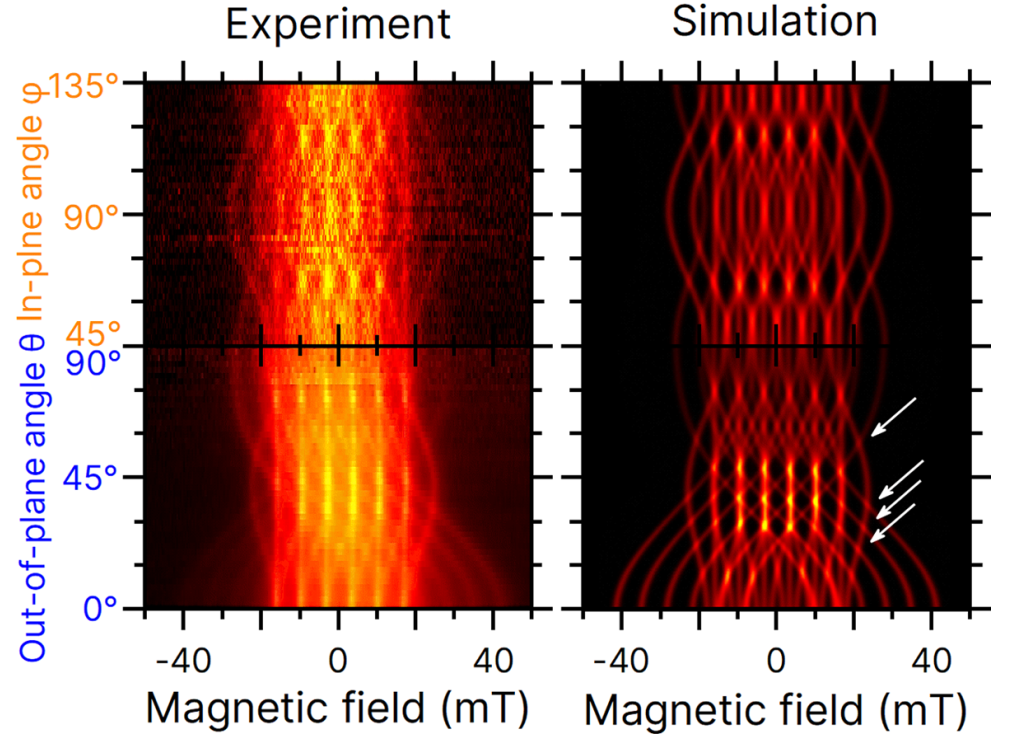
In this paper, we apply the angle-resolved optically detected magnetic resonance (ODMR) technique to study a series of strained (Cd, Mn)Te/(Cd, Mg)Te quantum wells (QWs) produced by molecular beam epitaxy. By analyzing characteristic features of ODMR angular scans, we determine the strain-induced axial-symmetry spin Hamiltonian parameter D with neV precision. Furthermore, we use low-temperature optical reflectivity measurements and x-ray diffraction scans to evaluate the local strain present in the QW material. In our analysis, we take into account different thermal expansion coefficients of the GaAs substrate and CdTe buffer. The additional deformation due to the thermal expansion effects has the same magnitude as the deformation that originates from the different compositions of the samples. Based on the evaluated deformations and values of the strain-induced axial-symmetry spin Hamiltonian parameter D, we find the strain spin-lattice coefficient G11=(72.2±1.9) neV for Mn2+ in CdTe and shear deformation potential b=(−0.94±0.11) eV for CdTe.
Polariton lasing and energy-degenerate parametric scattering in non-resonantly driven coupled planar microcavities
Krzysztof Sawicki, Thomas J. Sturges, Maciej Ściesiek, Tomasz Kazimierczuk, Kamil Sobczak, Andrzej Golnik, Wojciech Pacuski and Jan Suffczyński
Nanophotonics 10, no. 9, pp. 2421-2429 (2021)
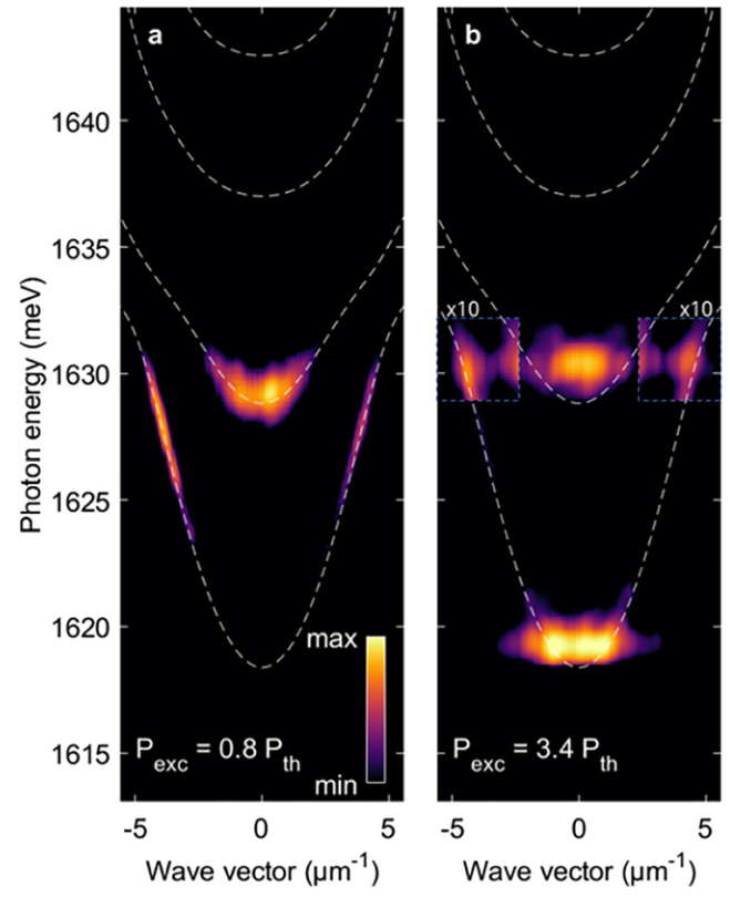
Multi-level exciton-polariton systems offer an attractive platform for studies of non-linear optical phenomena. However, studies of such consequential non-linear phenomena as polariton condensation and lasing in planar microcavities have so far been limited to two-level systems, where the condensation takes place in the lowest attainable state. Here, we report non-equilibrium Bose–Einstein condensation of exciton-polaritons and low threshold, dual-wavelength polariton lasing in vertically coupled, double planar microcavities. Moreover, we find that the presence of the non-resonantly driven condensate triggers interbranch exciton-polariton transfer in the form of energy-degenerate parametric scattering. Such an effect has so far been observed only under excitation that is strictly resonant in terms of the energy and incidence angle. We describe theoretically our time-integrated and time-resolved photoluminescence investigations by an open-dissipative Gross–Pitaevskii equation-based model. Our platform’s inherent tunability is promising for construction of planar lattices, enabling three-dimensional polariton hopping and realization of photonic devices, such as all-optical polariton-based logic gates.
__________________________________________________
Hybrid Semimagnetic Polaritons in a Strongly Coupled Optical Microcavity
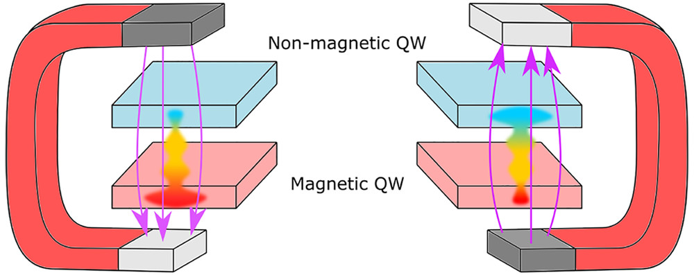
Exciton–polaritons of a hybrid type, emerging in a structure comprising semimagnetic (Mn-doped) and nonmagnetic quantum wells coupled via the microcavity optical mode are demonstrated and studied. Thanks to the susceptibility of the excitons in the magnetic quantum well to the magnetic field, all the emerging hybrid polariton states acquire magnetic properties. In that way, external magnetic field enables control over the degree of hybridization, tuning of the ratio of the excitonic to photonic components of the hybrid polaritons, and alteration of the direction and dynamics of the energy transfer between the excitonic states in magnetic and nonmagnetic quantum wells. The presented possibility of the hybridization of a semimagnetic exciton with an exciton in a material that itself does not exhibit any meaningful magnetic effects is highly promising in the context of the fabrication of—to date lacking—organic, perovskite, or dichalcogenide-based systems with strong magnetooptical properties.
Tomasz Fąs, Maciej Ściesiek, Wojciech Pacuski, Andrzej Golnik, and Jan Suffczyński, J. Phys. Chem. Lett. 12, 31, 7619–7624 (2021)
__________________________________________________
Local field effects in ultrafast light–matter interaction measured by pump-probe spectroscopy of monolayer MoSe2
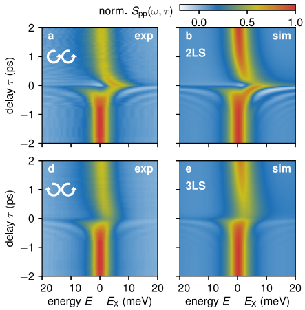
Using ultrafast resonant pump-probe spectroscopy in an unconventional experimental setup we investigate the spectral shape and dynamics of absorption features related to the A exciton in an hexagonal boron nitride (hBN)/MoSe2/hBN van der Waals heterostructure. While in a pure two-level system a pump-probe experiment measures the occupation or the polarization dynamics, depending on the time ordering of the pulse pair, in the transition metal dichalcogenide (TMD) system both quantities get thoroughly mixed by strong exciton–exciton interaction. We find that for short positive delays the spectral lines experience pronounced changes in their shape and energy and they relax to the original situation on a picosecond time scale. For negative delays, distinctive spectral oscillations appear indicating the first-time observation of perturbed free induction decay for a TMD system. The comparison between co-circular and cross-circular excitation schemes further allows us to investigate the rapid inter-valley scattering. By considering a three-level system as a minimal model including the local field effect, excitation-induced dephasing (EID), and scattering between the excited states we explain all phenomena observed in the experiment with excellent consistency. Our handy model can be even further reduced to two levels in the case of a co-circular excitation, for which we derive analytic expressions to describe the detected signals. This allows us to trace back the spectral shapes and shifts to the impact of local field effect and EID thus fully reproducing the complex behavior of the observed effects.
Aleksander Rodek, Thilo Hahn, Jacek Kasprzak, Tomasz Kazimierczuk, Karol Nogajewski, Karolina Połczyńska, Kenji Watanabe, Takashi Taniguchi, Tilmann Kuhn, Paweł Machnikowski, Marek Potemski, Daniel Wigger, Piotr Kossacki, Nanophotonics 10, 2717 (2021)
__________________________________________________
Long-distance coupling and energy transfer between exciton states in magnetically controlled microcavities
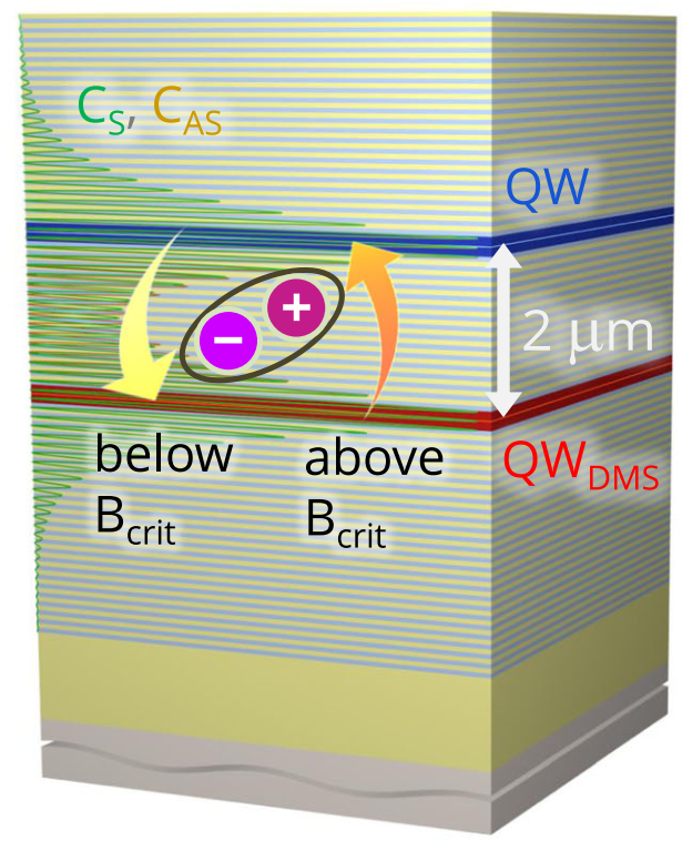
Coupling of quantum emitters in a semiconductor relies, generally, on short-range dipole-dipole or electronic exchange type interactions. Consistently, energy transfer between exciton states, that is, electron-hole pairs bound by Coulomb interaction, is limited to distances of the order of 10 nm. Here, we demonstrate polariton-mediated coupling and energy transfer between excitonic states over a distance exceeding 2 μm. We accomplish this by coupling quantum well-confined excitons through the delocalized mode of two coupled optical microcavities. Use of magnetically doped quantum wells enables us to tune the confined exciton energy by the magnetic field and in this way to control the spatial direction of the transfer. Such controlled, long-distance interaction between coherently coupled quantum emitters opens possibilities of a scalable implementation of quantum networks and quantum simulators based on solid-state, multi-cavity systems.
Maciej Ściesiek, Krzysztof Sawicki, Wojciech Pacuski, Kamil Sobczak, Tomasz Kazimierczuk, Andrzej Golnik and Jan Suffczyński, Commun Mater 1, 78 (2020)
__________________________________________________
Carrier relaxation to quantum emitters in few-layer WSe2
We present a detailed study of the time-resolved photoluminescence of narrow-line emission centers in WSe2 monolayers and bilayers. Our experiments reveal noninstantaneous photoluminescence intensity rise after the laser pulse. This shows that the simplest excitation model in which the localized states are directly populated by free excitons is not sufficient to fully reproduce experimental results. We, therefore, analyze a more complex phenomenological model where the relaxation of the carriers is mediated by long-lived intermediate states. Strong suppression of the lifetime of those intermediate states at elevated temperatures reveals their unique character, not matching any relaxed excitonic state in WSe2 monolayer. 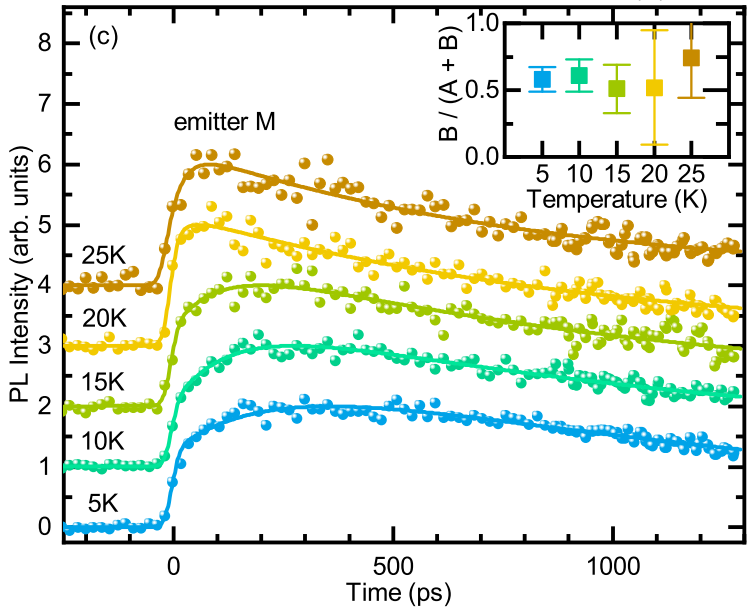
K. Oreszczuk, T. Kazimierczuk, T. Smoleński, K. Nogajewski, M. Grzeszczyk, A. Łopion, M. Potemski, and P. Kossacki, Phys. Rev. B 102, 245409 (2020)
__________________________________________________
Valley pseudospin relaxation of charged excitons in monolayer MoTe2
Zeeman effect induced by the magnetic field introduces a splitting between the two valleys at K+ and K− points of the Brillouin zone in monolayer semiconducting transition metal dichalcogenides. In consequence, the photoluminescence signal exhibits a field dependent degree of circular polarization. We present a comprehensive study of this effect in the case of a trion in monolayer MoTe2, showing that although time integrated data allows us to deduce a g-factor of the trion state, such an analysis cannot be substantiated by the timescales revealed in the time-resolved experiments. 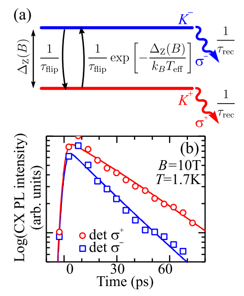
T. Smoleński, T. Kazimierczuk, M. Goryca, K. Nogajewski, M Potemski, and P. Kossacki, J. Phys.: Condens. Matter 33, 025701 (2020) https://arxiv.org/abs/2005.14095
__________________________________________________
Narrow excitonic lines and large scale homogeneity of transition metal dichalcogenide grown by MBE on hBN
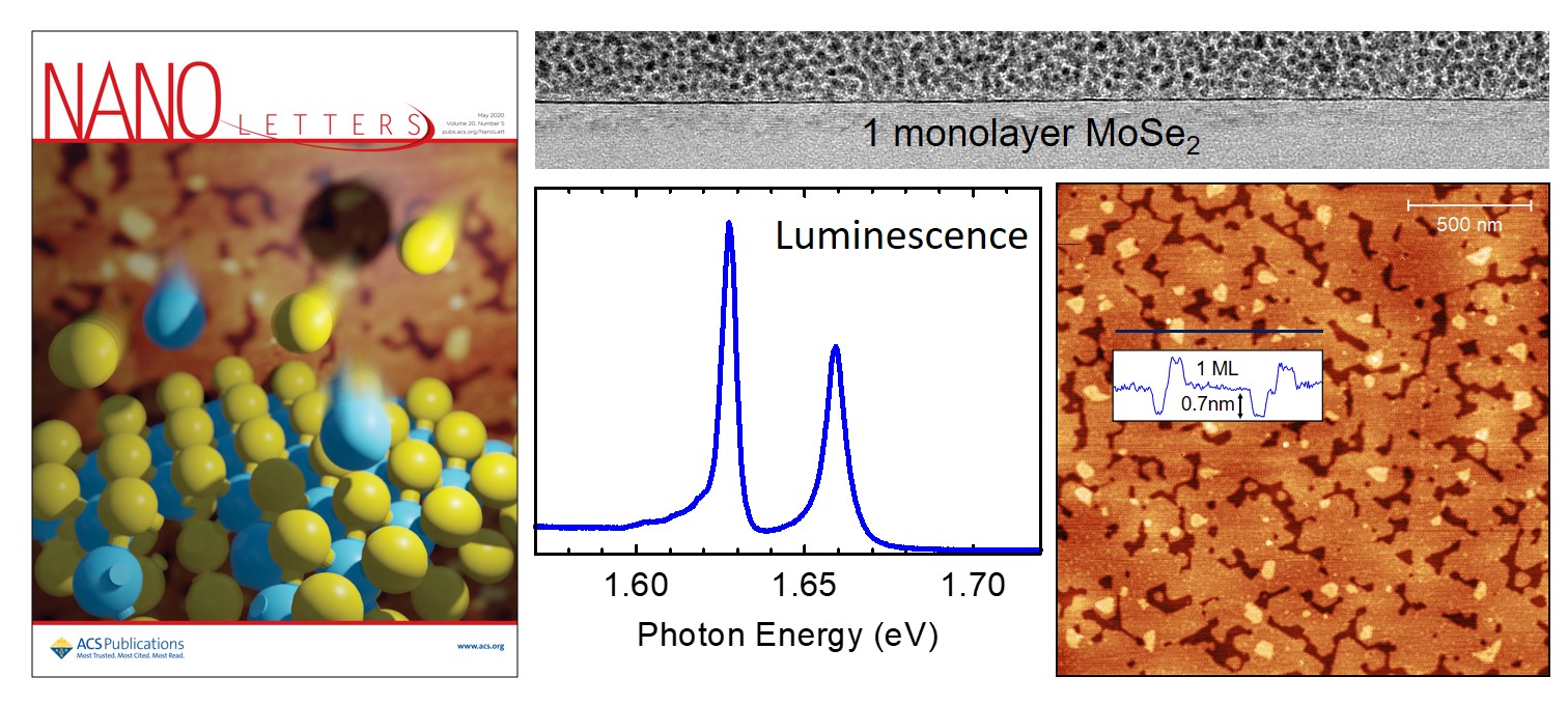
Monolayer transition-metal dichalcogenides (TMDs) manifest exceptional optical properties related to narrow excitonic resonances. However, these properties have been so far explored only for structures produced by techniques inducing considerable large-scale inhomogeneity. In contrast, techniques which are essentially free from this disadvantage, such as molecular beam epitaxy (MBE), have to date yielded only structures characterized by considerable spectral broadening, which hinders most of the interesting optical effects. Here, we report for the first time on the MBE-grown TMD exhibiting narrow and resolved spectral lines of neutral and charged exciton. Moreover, our material exhibits unprecedented high homogeneity of optical properties, with variation of the exciton energy as small as ±0.16 meV over a distance of tens of micrometers. Our recipe for MBE growth is presented for MoSe2 and includes the use of atomically flat hexagonal boron nitride substrate. This recipe opens a possibility of producing TMD heterostructures with optical quality, dimensions, and homogeneity required for optoelectronic applications.
W. Pacuski, M. Grzeszczyk, K. Nogajewski, A. Bogucki, K. Oreszczuk, J. Kucharek, K.E. Połczynska, B. Seredynski, R. Bozek, T. Taniguchi, K. Watanabe, J. Sadowski, T. Kazimierczuk, M. Potemski, and P. Kossacki Nano Lett. 20, 3058 (2020) https://doi.org/10.1021/acs.nanolett.9b04998
__________________________________________________
Ultra-long-working-distance spectroscopy of single nanostructures with aspherical solid immersion microlenses
In light science and applications, equally important roles are played by efficient light emitters/detectors and by the optical elements responsible for light extraction and delivery. The latter should be simple, cost effective, broadband, versatile and compatible with other components of widely desired micro-optical systems. Ideally, they should also operate without high-numerical-aperture optics. Here, we demonstrate that all these requirements can be met with elliptical microlenses 3D printed on top of light emitters. Importantly, the microlenses we propose readily form the collected light into an ultra-low divergence beam (half-angle divergence below 1°) perfectly suited for ultra-long-working-distance optical measurements (600 mm with a 1-inch collection lens), which are not accessible to date with other spectroscopic techniques. Our microlenses can be fabricated on a wide variety of samples, including semiconductor quantum dots and fragile van der Waals heterostructures made of novel two-dimensional materials, such as monolayer and few-layer transition metal dichalcogenides.
Aleksander Bogucki, Łukasz Zinkiewicz, Magdalena Grzeszczyk, Wojciech Pacuski, Karol Nogajewski, Tomasz Kazimierczuk, Aleksander Rodek, Jan Suffczyński, Kenji Watanabe, Takashi Taniguchi, Piotr Wasylczyk, Marek Potemski and Piotr Kossacki, Light: Science & Applications, 9, 48 (2020).
__________________________________________________
Direct measurement of hyperfine shifts and radiofrequency manipulation of the nuclear spins in individual CdTe/ZnTe quantum dots
We achieve direct detection of electron hyperfine shifts in individual CdTe/ZnTe quantum dots. For the previously inaccessible regime of strong magnetic fields Bz>0.1T, we demonstrate robust polarization of a few-hundred-particle nuclear spin bath, with an optical initialization time of 1ms and polarization lifetime exceeding 1s. Nuclear magnetic resonance spectroscopy of individual dots reveals strong electron-nuclear interactions characterized by Knight fields |Be|>50mT, an order of magnitude stronger than in III–V semiconductor quantum dots. Our studies confirm II–VI semiconductor quantum dots as a promising platform for hybrid electron-nuclear spin qubit registers, combining the excellent optical properties comparable to III–V dots and the dilute nuclear spin environment similar to group-IV semiconductors.

G. Ragunathan, J. Kobak, G. Gillard, W. Pacuski, K. Sobczak, J. Borysiuk, M. S. Skolnick, E. A. Chekhovich, Phys. Rev. Lett., 122, 096801 (2019).
__________________________________________________
Triple threshold lasing from a photonic trap in a Te/Se-based optical microcavity
Lasing relies on light amplification in the active medium of an optical resonator. There are three lasing regimes in the emission from a quantum well coupled to a semiconductor microcavity. Polariton lasing in the strong light–matter coupling regime arises from the stimulated scattering of exciton-polaritons. Photon lasing in the weak coupling regime relies on either of two mechanisms: the stimulated recombination of excitons, or of an electron–hole plasma. So far, only one or two out of these three regimes have been reported for a given structure, independently of the material system studied. Here, we report on all three lasing regimes and provide evidence for a three-threshold behavior in the emission from a photonic trap in a Se/Te-based planar microcavity comprising a single CdSe/(Cd,Mg)Se quantum well. Our work establishes the so far unsettled relation between lasing regimes that differ by their light-matter coupling strength and degree of electron–hole Coulomb correlation.
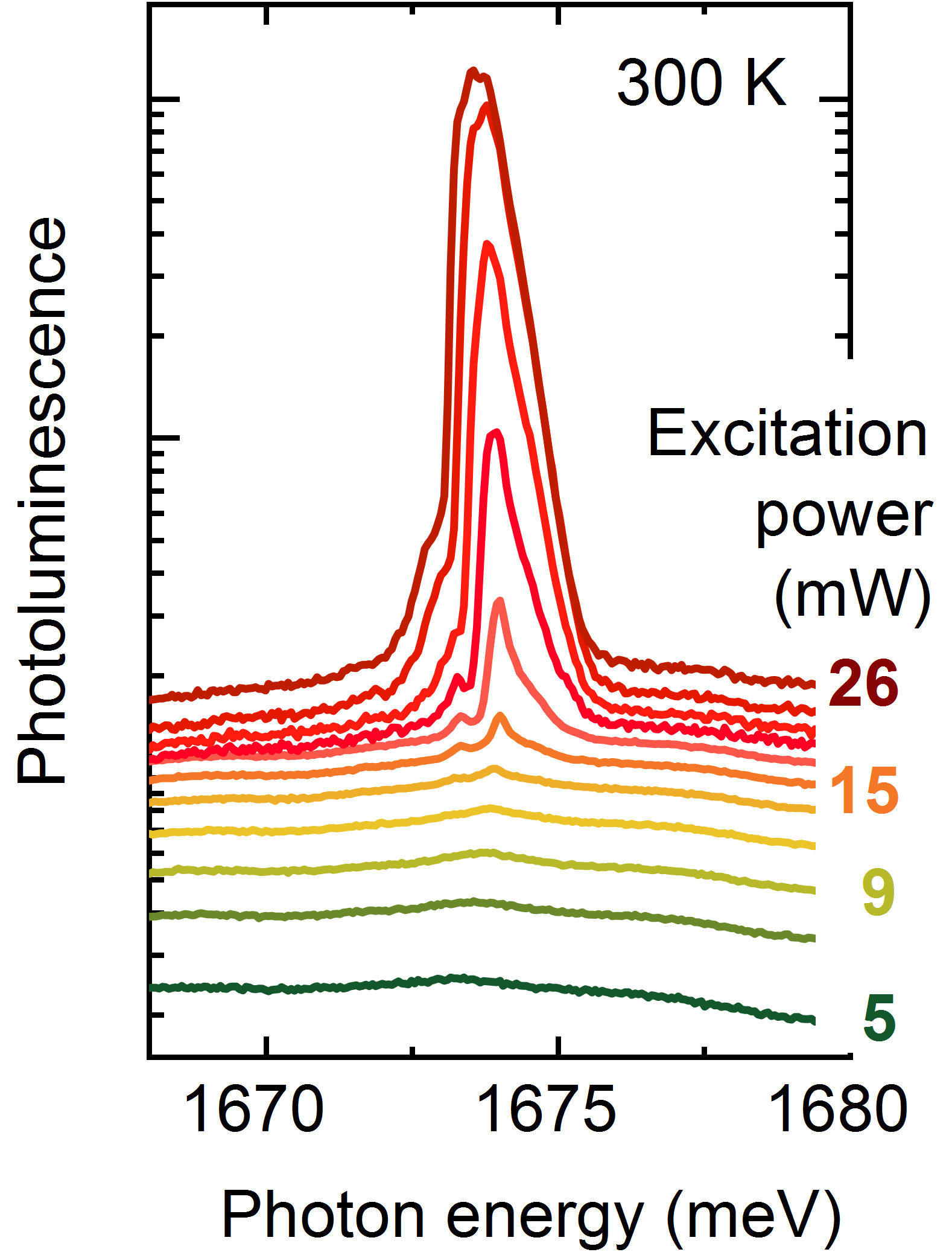
K. Sawicki, J-G. Rousset, R. Rudniewski, W. Pacuski, M. Ściesiek, T. Kazimierczuk, K. Sobczak, J. Borysiuk, M. Nawrocki, and J. Suffczyński, Communications Physics 2, 38 (2019)
__________________________________________________
Optical fiber micro-connector with nanometer positioning precision for rapid prototyping of photonic devices
Prototyping of fiber-coupled integrated photonic devices requires robust and reliable way of docking optical fibers to other structures, often with sub-micron accuracy. We have developed an optical fiber micro-connector 3D-printed with Direct Laser Writing on a planar substrate. The connector provides fiber core precision positioning better than 120 nm and sustains cryogenic cycling without any signs of degradation. It can be fabricated and used on glass and non-transparent substrates, including photonic integrated circuits, semiconductor samples, and microfluidic systems.
Aleksander Bogucki, Łukasz Zinkiewicz, Wojciech Pacuski, Piotr Wasylczyk, and Piotr Kossacki, Optics Express 262, 11513 (2018)
__________________________________________________
(Cd,Zn,Mg)Te-based microcavity on MgTe sacrificial buffer: Growth, lift-off, and transmission studies of polaritons
Opaque substrates precluded, so far, transmission studies of II-VI semiconductor microcavities. This work presents the design and molecular beam epitaxy growth of semimagnetic (Cd,Zn,Mn)Te quantum wells embedded into a (Cd,Zn,Mg)Te-based microcavity, which can be easily separated from the GaAs substrate. Our lift-off process relies on the use of a MgTe sacrificial layer which stratifies in contact with water. This allowed us to achieve a II-VI microcavity prepared for transmission measurements. We evidence the strong light-matter coupling regime using photoluminescence, reflectivity, and transmission measurements at the same spot on the sample. By comparing a series of reflectance spectra before and after lift-off, we prove that the microcavity quality remains high. Thanks to Mn content in quantum wells we show the giant Zeeman splitting of semimagnetic exciton-polaritons in our transmitting structure.
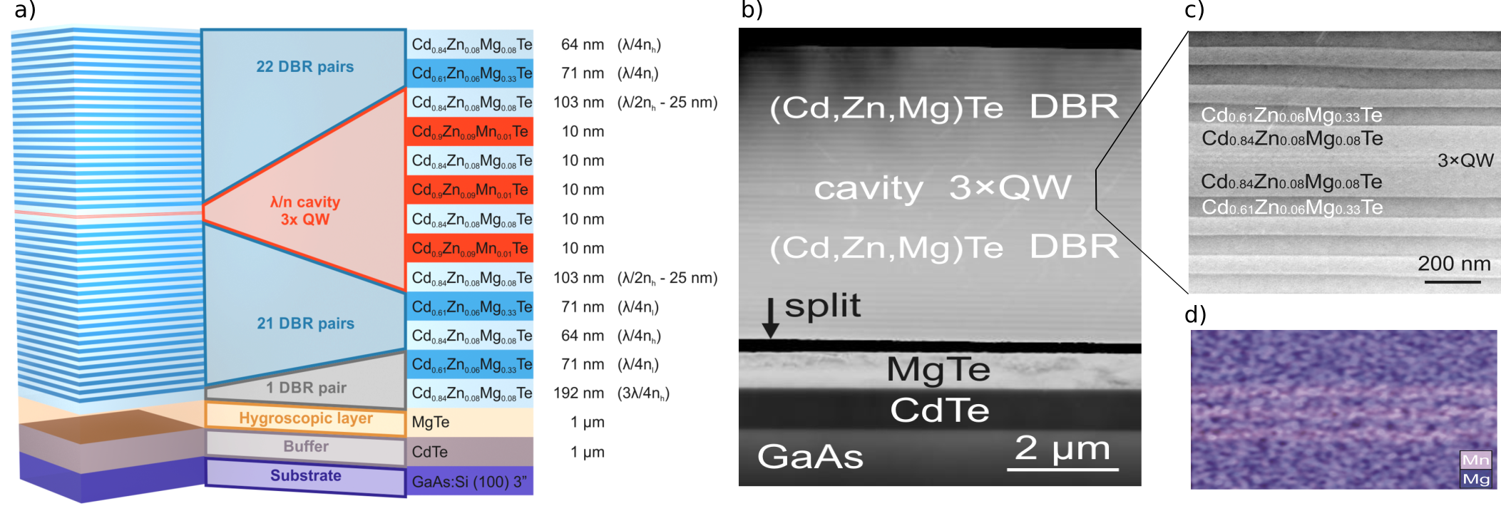
B. Seredyński, M. Król, P. Starzyk, R. Mirek, M. Ściesiek, K. Sobczak, J. Borysiuk, D. Stephan, J.-G. Rousset, J. Szczytko, B. Piętka, W. Pacuski,Phys. Rev. Materials 2, 043406 (2018).
__________________________________________________
Tuning Valley Polarization in a WSe2 Monolayer with a Tiny Magnetic Field
In monolayers of semiconducting transition metal dichalcogenides, the light helicity (σ+ or σ−) is locked to the valley degree of freedom, leading to the possibility of optical initialization of distinct valley populations. However, an extremely rapid valley pseudospin relaxation (at the time scale of picoseconds) occurring for optically bright (electric-dipole active) excitons imposes some limitations on the development of opto-valleytronics. Here, we show that valley pseudospin relaxation of excitons can be significantly suppressed in a WSe2 monolayer, a direct-gap two-dimensional semiconductor with the exciton ground state being optically dark. We demonstrate that the already inefficient relaxation of the exciton pseudospin in such a system can be suppressed even further by the application of a tiny magnetic field of about 100 mT. Time-resolved spectroscopy reveals the pseudospin dynamics to be a two-step relaxation process. An initial decay of the pseudospin occurs at the level of dark excitons on a time scale of 100 ps, which is tunable with a magnetic field. This decay is followed by even longer decay (>1 ns), once the dark excitons form more complex pseudo-particles allowing for their radiative recombination. Our findings of slow valley pseudospin relaxation easily manipulated by the magnetic field open new prospects for engineering the dynamics of the valley pseudospin in transition metal dichalcogenides.

T. Smoleński, M. Goryca, M. Koperski, C. Faugeras, T. Kazimierczuk, A. Bogucki, K. Nogajewski, P. Kossacki, and M. Potemski
Physical Review X 6, 021024 (2016)
__________________________________________________ 
Magnetic ground state of an individual Fe2+ ion in strained semiconductor nanostructure
Single impurities with nonzero spin and multiple ground states offer a degree of freedom that can be utilized to store the quantum information. However, Fe2+ dopant is known for having a single nondegenerate ground state in the bulk host semiconductors and thus is of little use for spintronic applications. Here we show that the well-established picture of Fe2+ spin configuration can be modified by subjecting the Fe2+ ion to high strain, for example, produced by lattice mismatched epitaxial nanostructures. Our analysis reveals that high strain induces qualitative change in the ion energy spectrum and results in nearly doubly degenerate ground state with spin projection Sz=±2. We provide an experimental proof of this concept using a new system: a strained epitaxial quantum dot containing individual Fe2+ ion. Magnetic character of the Fe2+ ground state in a CdSe/ZnSe dot is revealed in photoluminescence experiments by exploiting a coupling between a confined exciton and the single-iron impurity. We also demonstrate that the Fe2+ spin can be oriented by spin-polarized excitons, which opens a possibility of using it as an optically controllable two-level system free of nuclear spin fluctuations.
T. Smoleński, T. Kazimierczuk, J. Kobak, M. Goryca, A. Golnik, P. Kossacki and W. Pacuski, Nature Communications 7, 10484 (2016)
__________________________________________________
Single photon emitters in exfoliated WSe2 structures
Crystal structure imperfections in solids often act as efficient carrier trapping centres, which, when suitably isolated, act as sources of single photon emission. The best known examples of such attractive imperfections are well-width or composition fluctuations in semiconductor heterostructures1, 2 (resulting in the formation of quantum dots) and coloured centres in wide-bandgap materials such as diamond3, 4, 5. In the recently investigated thin films of layered compounds, the crystal imperfections may logically be expected to appear at the edges of commonly investigated few-layer flakes of these materials exfoliated on alien substrates. Here, we report comprehensive optical micro-spectroscopy studies of thin layers of tungsten diselenide (WSe2), a representative semiconducting dichalcogenide with a bandgap in the visible spectral range. At the edges of WSe2 flakes (transferred onto Si/SiO2 substrates) we discover centres that, at low temperatures, give rise to sharp emission lines (100 μeV linewidth). These narrow emission lines reveal the effect of photon antibunching, the unambiguous attribute of single photon emitters. The optical response of these emitters is inherently linked to the two-dimensional properties of the WSe2 monolayer, as they both give rise to luminescence in the same energy range, have nearly identical excitation spectra and have very similar, characteristically large Zeeman effects. With advances in the structural control of edge imperfections, thin films of WSe2 may provide added functionalities that are relevant for the domain of quantum optoelectronics.

M. Koperski, K. Nogajewski, A. Arora, V. Cherkez, P. Mallet, J.-Y. Veuillen, J. Marcus, P. Kossacki and M. Potemski, Nature Nanotechnology10, 503 (2015)
__________________________________________________
Designing quantum dots for solotronics
Solotronics, optoelectronics based on solitary dopants, is an emerging field of research and technology reaching the ultimate limit of miniaturization. It aims at exploiting quantum properties of individual ions or defects embedded in a semiconductor matrix. It has already been shown that optical control of a magnetic ion spin is feasible using the carriers onfined in a quantum dot. However, a serious obstacle was the quenching of the exciton luminescence by magnetic impurities. Here we show, by photoluminescence studies on thus-far-unexplored individual CdTe dots with a single cobalt ion and CdSe dots with a single manganese ion, that even if energetically allowed, nonradiative exciton recombination through single-magnetic-ion intra-ionic transitions is negligible in such zero-dimensional structures. This opens solotronics for a wide range of as yet unconsidered systems. On the basis of results of our single-spin relaxation experiments and on the material trends, we identify optimal magnetic-ion quantum dot systems for implementation of a single-ion-based spin memory.

J. Kobak, T. Smoleński, M. Goryca, M. Papaj, K. Gietka, A. Bogucki, M. Koperski, J.-G. Rousset, J. Suffczyński, E. Janik, M. Nawrocki,
A. Golnik, P. Kossacki, and W. Pacuski, Nature Communications 5, 3191 (2014).
__________________________________________________ 
Coherent Precession of an Individual 5/2 Spin
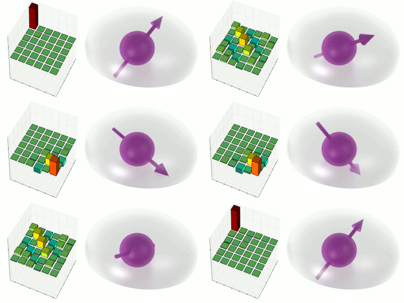
We present direct observation of a coherent spin precession of an individual Mn2+ ion, having both electronic and nuclear spins equal to 5/2, embedded in a CdTe quantum dot and placed in a magnetic field. The spin state evolution is probed in a time-resolved pump-probe measurement of absorption of the single dot. The experiment reveals subtle details of the large-spin coherent dynamics, such as nonsinusoidal evolution of states occupation, and beatings caused by the strain-induced differences in energy levels separation. Sensitivity of the large-spin impurity on the crystal strain opens the possibility of using it as a local strain probe.
M. Goryca, M. Koperski, P. Wojnar, T. Smoleński, T. Kazimierczuk, A. Golnik, and P. KossackiPhysical Review Letters 113, 227202 (2014)
__________________________________________________
Inhibition and Enhancement of the Spontaneous Emission of Quantum Dots in Micropillar Cavities with Radial-Distributed Bragg Reflectors
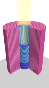
We present a micropillar cavity where nondesired radial emission is inhibited. The photonic confinement in such a structure is improved by implementation of an additional concentric radial-distributed Bragg reflector. Such a reflector increases the reflectivity in all directions perpendicular to the micropillar axis from a typical value of 15–31% to above 98%. An inhibition of the spontaneous emission of off-resonant excitonic states of quantum dots embedded in the microcavity is revealed by time-resolved experiments. It proves a decreased density of photonic states related to unwanted radial leakage of photons out of the micropillar. For on-resonance conditions, we find that the dot emission rate is increased, evidencing the Purcell enhancement of spontaneous emission. The proposed design can increase the efficiency of single-photon sources and bring to micropillar cavities the functionalities based on lengthened decay times.
